Optical spectroscopy of Moiré homo and heterostructures
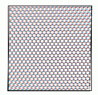
Vertical homo and heterostructures are thought to be van der Waals bound (weak binding), but recent studies suggest that layers may be coupled more strongly, and may also go beyond the rigid lattice picture. Further, the twist angle between layers imparts a tunable moiré period, scaling as (unit cell length)/(twist angle), leading to a modified potential landscape. These moiré heterostructures emerge as an ideal platform to realise new properties and functionalities that are not present in the individual layers. Additionally, the moiré potentials give rise to well defined localized moiré excitons (interlayer and intralayer excitons), that are protected against disorder, and can be tuned with external fields revealing interesting topological phases, many-body interactions, and quantum phase transitions. Optical techniques are ideal to explore these systems due to their strong interaction with light. Using both steady-state and time-resolved optical spectroscopies such as steady-state and time-resolved photoluminescence (TRPL) and transient absorption (Pump-Probe) spectroscopy, we study inter-layer coupling, spin-valley information and fundamental carrier dynamics, which occur over timescales of femtoseconds-nanoseconds.
Useful references:
Mondal et al., Quantification of 2D Interfaces: Quality of heterostructures, and what is inside a nanobubble, ACS Applied Materials and Interfaces 16 42608 (2024)
Debnath et al., “Tuning exciton complexes in twisted bilayer WSe2 at intermediate misorientation”, Physical Review B 106 125409 (2022)
Tran et al., “Moiré and beyond in transition metal dichalcogenide twisted bilayers”, 2DMater. 8 022002 (2021)
Tran et al., “Evidence for moiré excitons in van der Waals heterostructures”, Nature 567, 71-75 (2019)