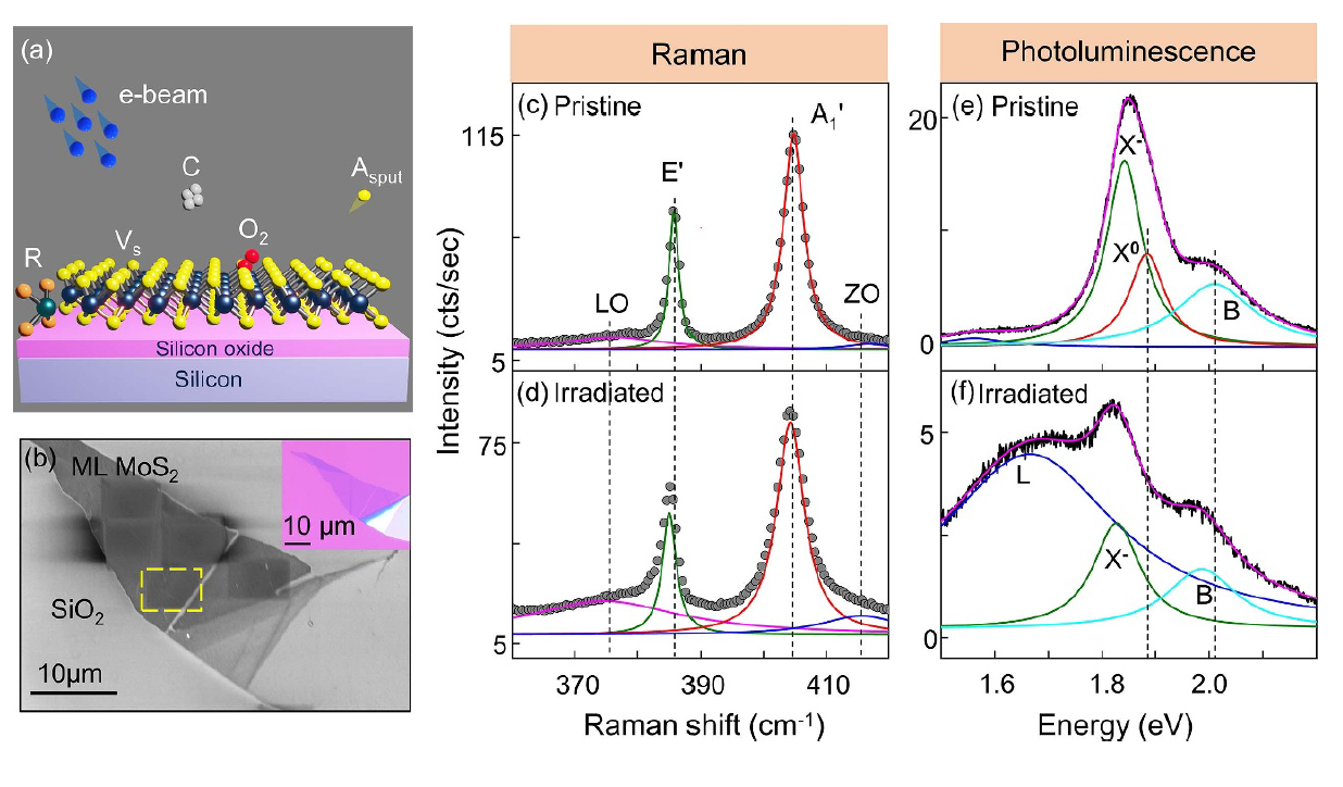
Control on spatial location and density of defects in two-dimensional materials can be achieved using electron beam irradiation. Conversely, ultralow accelerating voltages (⩽5 kV) are used to measure surface morphology, with no expected defect creation. We find clear signatures of defect creation in monolayer MoS2 at these voltages. Evolution of E ′ and A ′ Raman modes with electron dose, and appearance of defect activated peaks indicate defect formation. To simulate Raman spectra of MoS2 at realistic defect distributions, while retaining density-functional theory accuracy, we combine machine-learning force fields for phonons and eigenmode projection approach for Raman tensors. Simulated spectra agree with experiments, with sulphur vacancies as suggested defects. We decouple defects, doping and carbonaceous contamination using control (hBN covered and encapsulated MoS2) samples. We observe cryogenic photoluminescence quenching and defect peaks, and find that carbonaceous contamination does not affect defect creation. These studies have applications in photonics and quantum emitters.
Paper available at: https://doi.org/10.1088/2053-1583/acc7b6 and https://arxiv.org/abs/2210.04662