Transport in ultra-thin nanowires

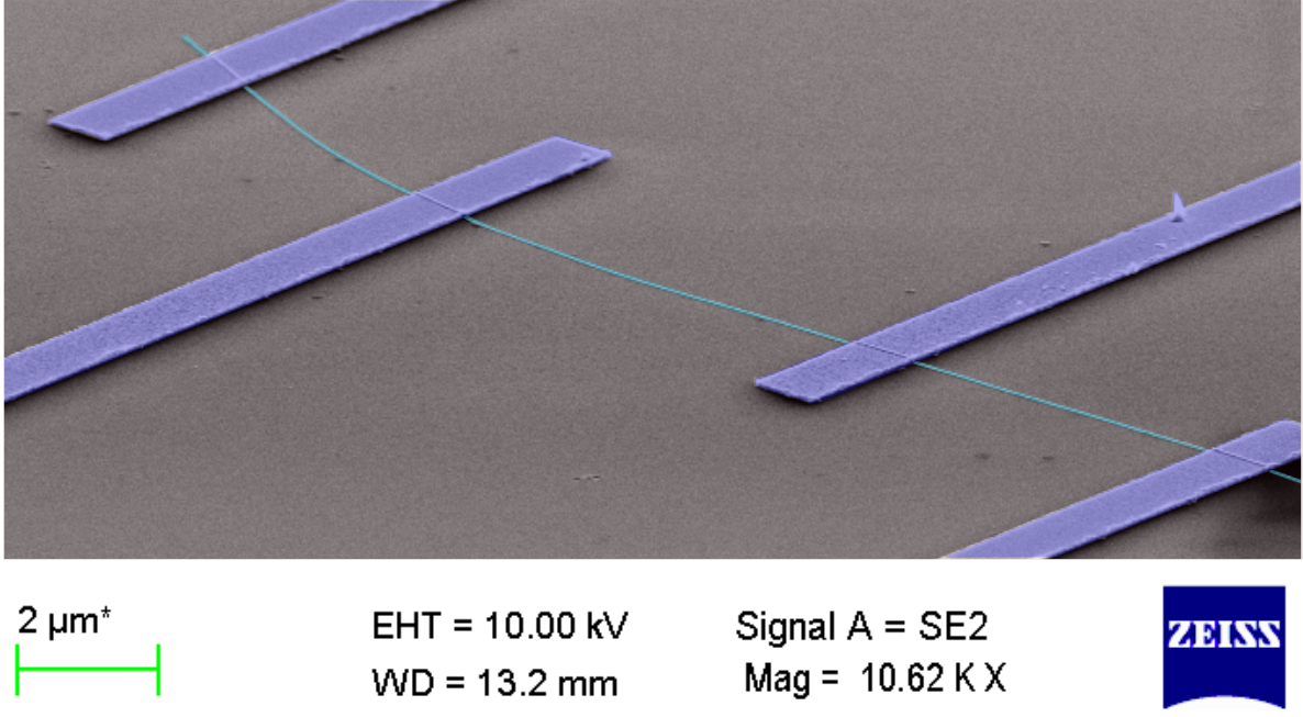
Te nanowire: We study electrical transport properties in semiconducting ultra thin tellurium nanowires. Pristine tellurium nanowire have band gap at fermi energy, and thus the transport is thermally activated in high temperature, followed by variable range hopping in low temperature. We have studied transport in single nanowire devices while exposing the nanowires with controlled amount of NO2. Ab. initio simulations showed that mid-gap state appears in presence of NO2 adsorbed on the surface of tellurium nanowire. This theoretical prediction of band structure modification was experimentally studied. The appearance of midgap states causes drop in electrical resistance of the nanowires. The temperature dependant transport showed decrease in activation energy and increase in localization length (ξ) while the nanowires were exposed with increasing concentration of NO2. Eventually, a metallic state of the nanowires is observed. The characteristic raman peaks of tellurium nanowires eventually quench with increasing amount of NO2 adsorption. This surface adsorption induced band structure engineering and semiconducting-metal transition allows tunability of opto-electronic properties of nanowires, which is extremely significant from both fundamental and application point of view.


Au nanowire: We have performed systematic studies of the dynamics of surface adsorption of various chemicals on ultra-thin single crystalline gold nanowires through sensitive resistance fluctuation spectroscopy measurements coupled with ab initio simulations. We show that, contrary to expectations, the adsorption of common chemicals like methanol and acetone have a profound impact on the electrical transport properties of the gold nanowires. Our measurements and subsequent calculations establish conclusively that in gold nanowires, semiconductor-like sensitivity to the ambient arises because of changes induced in its local density of states by the surface adsorbed molecules. The extreme sensitivity of the resistance fluctuations of the gold nanowires to ambient suggests their possible use as solid-state sensors.

VO2 nanowire: Vanadium dioxide is a strongly correlated material with a thermally driven, first-order metal–insulator transition well above room temperature (341K). Metal–insulator transition in VO2 is accompanied by the structural transformation of the crystalline lattice from a high symmetry tetragonal rutile metallic phase with uniform V-V bond distance of 2.85 A to a lower symmetry insulating monoclinic phase with dimerized molecular [VO6]-[VO6] pair exhibiting alternative V-V bond lengths of 2.65A and 3.12A. It is found that electrostatic charging at a surface drives all the previously localized charge carriers in the bulk material into motion, leading to the emergence of a three-dimensional metallic ground state. This non-local switching of the electronic state is achieved by applying a voltage of only about one volt. In a voltage-sweep measurement, the first-order nature of the metal–insulator transition provides a non-volatile memory effect. We have fabricated on substrate and suspended device with single VO2 nanobeam by electron beam lithography and studied the thermally and electrically driven metal insulator transition on electrical transport measurement and found out this metallic state on Raman spectroscopy occurred as a function of temperature. We are probing the unresolved mechanism of metal–insulator transition through detailed temperature and bias dependence of the statistics of conductance fluctuations in this system.

